P8X 8-Slot Backplane — Design Notes
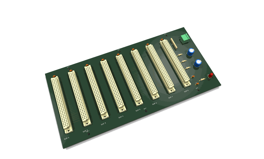
The board as routed in KiCad (3D render; top view).
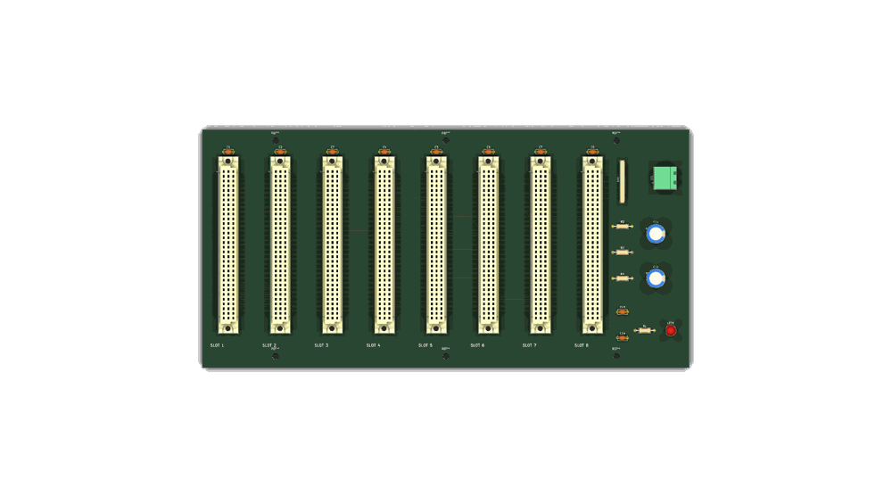
Theory of operation: p8x-backplane-theory.md — deep walkthrough of the bus map, signal integrity, and power.
Built version: the go-forward board is the KiCad build in
kicad/— 8 slots, 28 mm pitch, 262 × 128 mm, routed at 0.13 mm clearance, nylon-screw mounting. The layout figures below are the older Eagle rev-C notes (25.4 mm pitch, 10 slots); the bus pinout/theory still applies, only the slot count and physical layout changed.
1. Bus Pinout
The authoritative human-readable bus pinout is in p8x-bus-definition.md,
which is generated from the same busnet() function as the Eagle CAD files.
The machine-authoritative source is generators/gen_eagle.py.
Summary for quick reference (rev C2):
| Pin | Row A | Row B | Row C |
|---|---|---|---|
| 1–2 | +5V | +5V | +5V |
| 3–10 | D0–D7 | GND/SPARE (alt) | A0–A7 |
| 11 | -RES | GND/SPARE (alt) | A8 |
| 12–15 | DOE0–3 | GND/SPARE (alt) | A9–A12 |
| 16–19 | DLD0–3 | GND/SPARE (alt) | A13–A15, ALUS0 |
| 20–21 | PSEL0–1 | GND/SPARE (alt) | ALUS1–2 |
| 22–23 | PINC, PDEC | GND/SPARE (alt) | ALUS3, ALUM |
| 24–25 | CLK, CLKB | GND/SPARE (alt) | CIN, SH0 |
| 26–27 | LDF, FC | GND/SPARE, CLRC | SH1, PSEL2 |
| 28–30 | FZ, FN, FV | BSEL, IRQ, SPARE11 | LDZN, SHCIN, SETC |
| 31–32 | GND | GND | GND |
A27–A30 = FC/FZ/FN/FV (flag lines; were SPARE0–3 in rev C1). rev C3: C27–C30 = PSEL2/LDZN/SHCIN/SETC and B27 = CLRC (were SPARE4–8). rev C: B28 = BSEL (ALU B-input mux select, was SPARE9), B29 = IRQ (interrupt request, was SPARE10); SPARE11 remains on B30. rev D: B3–B26 alternate — odd pins stay GND (guard between signal pairs), even pins (B4,B6,…,B26) are spare bus lines SPARE12–SPARE23, routed slot-to-slot for future expansion without a backplane re-spin. See p8x-bus-definition.md for the authoritative per-pin map.
Signal positions are unchanged from rev B wherever they existed, so only the power pins moved. Rev B cards are incompatible (rev B grounded B2; rev C puts +5V there). The memory card schematic has been regenerated as rev C.
Current budget: DIN 41612 pins are rated ~2 A each → 6 parallel +5V pins and ~18 ground pins (the 6 pins on rows 31–32 plus the 12 odd-pin B-row guards; rev D reassigned the 12 even B-row pins from GND to spare lines) carry a 3–4 A system with comfortable margin and low connector drop.
2. PCB Construction — this is where the crosstalk battle is won
Use a 4-layer board. At today's fab prices the upcharge is small and it buys more than any other single decision:
| Layer | Content |
|---|---|
| L1 (top) | Signal: row A nets |
| L2 | Solid GND plane — no splits, no routing |
| L3 | Solid +5V plane |
| L4 (bottom) | Signal: row C nets |
This answers the "thicker power traces" requirement in the strongest possible way: the power distribution is two solid copper sheets (use 1 oz minimum, 2 oz if offered cheaply). It also gives every signal a tight return path, which is the primary crosstalk mechanism on a backplane — crosstalk is mostly a shared-return-inductance problem, and a plane under every trace mostly dissolves it.
Layout rules: - Slot pitch 25.4 mm (1.0"), 10 slots → board ≈ 275 × 110 mm - Bus traces run straight connector-to-connector, 0.3–0.4 mm width, ≥ 0.4 mm gaps; with the plane underneath, adjacent-trace coupling over these lengths is negligible at this technology's edge rates - Do not route signals between the planes or split the planes. Spares route like signals - CLK and CLKB get the royal treatment: route them with a ground trace on each side (guard traces) or with one empty channel between them and neighbors; keep them on one layer end to end - Decoupling: one 100 nF within 10 mm of each slot's power pins (C1–C10 in the schematic), 2 × 470 µF bulk near the power entry (C11/C12) - Power entry (J11, 4-pos screw terminal: 2 × +5V, 2 × GND) at one end; via-stitch generously into the planes (≥ 8 vias per terminal) - Stitch the row-B ground pins straight down into L2 at every slot — 280 ground vias distributed along the bus is a beautifully low-inductance grid - Power LED (R1 + LED1) so a dead PSU is diagnosed from across the room
If you must do 2-layer: top = signals + 10 mm power rails along each edge, bottom = ground pour flooded around a minimal number of crossing traces. It will work at 2 MHz. The 4-layer board will work at 8 MHz. Choose accordingly.
3. Termination — analysis and recommendation
The physics: the bus is ~23 cm. Unloaded propagation ≈ 1.5 ns end-to-end, but ten connector/card capacitive loads roughly double the effective delay and drop the loaded impedance to ~30–50 Ω. Round trip ≈ 5–7 ns. 74HCT edges are 3–5 ns — comparable to the round trip, which puts the bus at the edge of the transmission-line regime: you'll see some ringing on a scope, but at 2–4 MHz there are hundreds of nanoseconds for it to settle before anything is clocked. Termination is not required for functional correctness at the design speed. The ranked list of what actually prevents trouble:
- Ground plane + row-B guard grounds (overwhelmingly the biggest factor)
- Pull-ups on the data bus — RN1 (8 × 10 k) in the schematic. Not a termination at all, but essential with HCT: DOE=0 leaves D0–D7 undriven, and floating CMOS inputs oscillate and burn power. 10 k parks idle lines at a legal high
- Clean clock distribution (guard traces; optionally a 33 Ω series resistor at the clock driver on the control card to soften the launched edge)
Why classic passive (Thevenin) termination is wrong for this bus: the 220/330 Ω pairs on S-100 and Multibus backplanes bias undriven lines to ~2 V — fine for LS-TTL inputs, but 2 V is dead in the middle of an HCT input's threshold region, recreating the floating-input problem on purpose, plus ~25 mA of standing current per terminated line. Don't copy it onto an HCT bus.
Active termination (a regulated ~2.7 V rail feeding ~120 Ω per line — the SCSI approach) fixes Thevenin's power waste but keeps the mid-threshold bias problem for CMOS and adds a regulator. Justifiable on a long, fast, heavily-loaded bus; overkill by an order of magnitude here.
What the board provisions instead — AC (RC) termination on the two lines that merit it: CLK and CLKB each get 100 Ω + 150 pF to ground at the far end of the bus (R2/C13, R3/C14). AC termination damps reflections during edges but draws zero DC and imposes no bias level — the CMOS-friendly choice. Assembly guidance: leave them unpopulated at first. Bring the machine up, probe CLK at the far slot, and fit them only if you see ringing that crosses threshold regions. Footprints cost nothing; debugging mystery double-clocks costs weekends. If data/strobe lines ever ring problematically at higher clock speeds, the same RC treatment applies — but expect the planes to have already solved it.
4. Backplane BOM
| Ref | Part |
|---|---|
| J1–J10 | DIN 41612 96-pin female, vertical/press-fit or solder |
| J11 | 4-pos screw terminal, 5.08 mm |
| C11, C12 | 470 µF 10 V electrolytic |
| C1–C10 | 100 nF ceramic disc |
| RN1 | 10 kΩ × 8 bussed SIP-9 |
| R2, R3 | 100 Ω ¼ W (DNP initially) |
| C13, C14 | 150 pF ceramic (DNP initially) |
| R1, LED1 | 1 kΩ + 5 mm LED |
Footprint caveat: verify the exact KiCad footprint names for your female
DIN 41612 connectors (Connector_DIN:DIN41612_C_3x32_Female_Vertical is
assigned) against the parts in your stock — press-fit vs solder tail and
A/B/C pad naming vary by manufacturer.