Memory Card¶
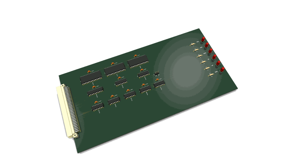
The board as routed in KiCad (3D render; top view).
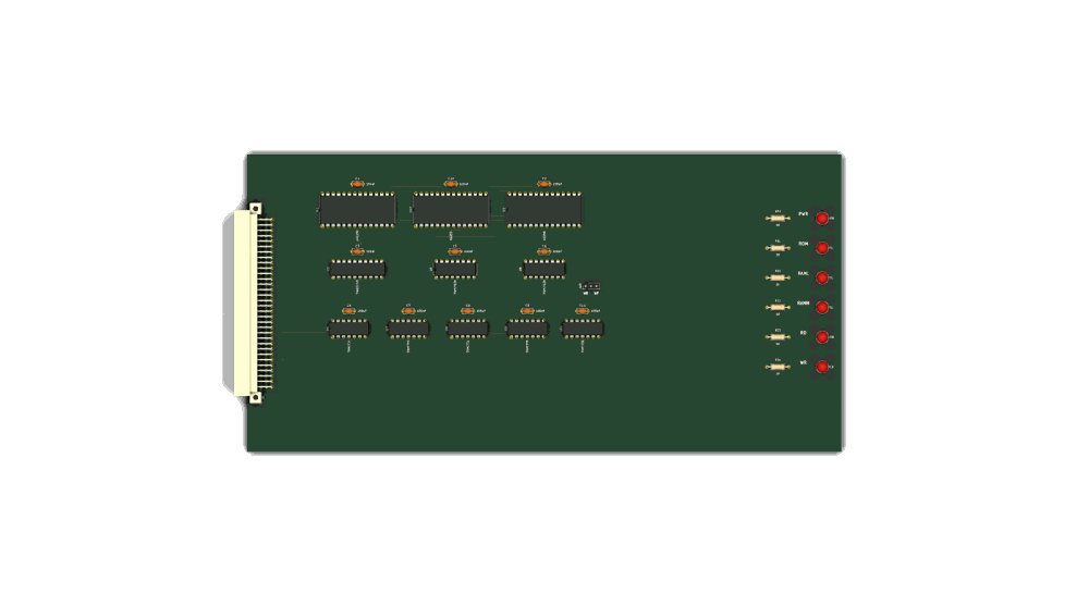
Theory of operation: p8x-memory-card-theory.md — deep walkthrough of inputs/outputs, signal flow, and logic.
Provides the system's ROM and RAM and gates them onto the data bus. It decodes the address bus to pick ROM vs RAM, keeps both off the data bus during I/O accesses, and generates a clean write strobe.
Build the KiCad rev F board. The 2026-09-14 ROM shrink made the map 6 KB ROM
$0000–$17FFwith$1800–$1FFFa RAM scratch island (written by the OS/BIOS, so it must be RAM). The KiCad board inkicad/(rev F, routed, not yet fabricated) implements that decode on three spare gates, with no new chips: ROM!CEgains anA11·A12term and low-RAM U10 widens to$1800–$7FFF. The chip-by-chip text below describes the rev E netlist ingen_eagle.py(8 KB ROM,$0000–$1FFF), whichkicad/gen_mem.pyimports and rewires to rev F; the frozen Eagle.schineagle-deprecated/is rev E too and must not be built.
| Region | Device | Size |
|---|---|---|
$0000–$17FF |
28C64 ROM (U1) | 6 KB — monitor + BIOS (BASIC is a disk program) |
$1800–$1FFF |
62256 SRAM (U10) | 2 KB scratch island (IBUF/SBUF/BIOS scratch) |
$2000–$7FFF |
62256 SRAM (U10) | 24 KB |
$8000–$FEFF |
62256 SRAM (U2) | 32 KB (minus the I/O page) |
$FF00–$FFFF |
— (I/O page) | RAM inhibited; handled by I/O & CF cards |
(Rev E after the 2026-09-14 shrink: 6 KB ROM at $0000–$17FF; two 62256 cover
$1800–$FEFF = 58 KB; OS loads at $2000.)
This README describes the circuit as actually built in
generators/gen_eagle.py. See p8x-system-design.md §6 for the overview and p8x-bus-definition.md for bus pins.
Chip inventory¶
| Ref | Device | Role |
|---|---|---|
| U1 | 28C256 (low 8 KB used; or a 28C64) | ROM (rev E: 8 KB, $0000–$1FFF; rev F: 6 KB, $0000–$17FF) |
| U2 | 62256 | SRAM, 32 KB ($8000–$FEFF) |
| U10 | 62256 | SRAM, 24 KB ($2000–$7FFF, rev E; $1800–$7FFF in rev F) |
| U3 | 74245 | Bidirectional data-bus transceiver |
| U4 | 7430 | 8-input NAND — I/O page ($FFxx) detector |
| U5 | 74138 | DOE decoder (read enable) |
| U6 | 74138 | DLD decoder (write strobe) |
| U7 | 74HCT00 | NAND — RAM chip-select logic |
| U8 | 74HCT32 | OR — write-strobe gating |
| U9 | 74HCT08 | AND — transceiver enable (rev F: spare gate U9.4 = A11·A12) |
| U11 | 74HCT32 | OR — ROM !CE (rev E: A13 OR A14 OR A15; rev F adds the A11·A12 term on U11.2/U11.3) |
How it works¶
Address decode (ROM vs RAM vs I/O) — rev E, decoded from A13 + A14 + A15¶
- ROM (U1) is selected when A13 = A14 = A15 = 0 —
!CE = A13 OR A14 OR A15, so the ROM responds for$0000–$1FFF(8 KB). - Low RAM (62256, U10) is selected when A15 = 0 and (A13 or A14) = 1 —
!CE = A15 OR NOR(A13, A14), covering$2000–$7FFF(deselected in the$0000–$1FFFROM page). - The I/O page detector (U4, a 7430 8-input NAND on A8–A15) asserts
-IOPGlow whenever the address is$FFxx. - Main RAM (62256, U2) is selected only when A15 = 1 and not the I/O page.
U7 NANDs A15 with
-IOPGto produce-RAMCE: RAM enables for$8000–$FEFFbut stays off for$FFxx, leaving that page to the I/O and CF cards.
The rev-E decode adds the A13 term to the ROM/RAM-low select. rev D's spare gates
were used up, so rev E adds exactly one 2-input gate: U11.1 (a 74HCT32 OR).
The rev-D gates are reused in place — U8.4 now ORs A13,A14 into Q; U11.1
ORs Q with A15 for the ROM !CE (A13|A14|A15); and U7.3 NANDs !A15 with
Q for the RAM-low !CE (= A15 OR NOR(A13,A14)). U11's 100 nF cap is C11.
Data-bus transceiver¶
The 74245 (U3) connects on-card memory to the backplane data bus. Its direction
is set by read vs write: on a read (DOE = 7 → -RD) it drives the bus from memory;
on a write (DLD = 7 → -MEMW) it drives memory from the bus. It is enabled only
for on-card addresses (-BOE, gated in U9), so the card never fights another
driver during I/O cycles.
Read path¶
DOE code 7 (-RD, decoded by U5) drives the memory output-enables (!OE) and sets
the 74245 direction toward the bus. The selected chip (ROM or RAM, per the decode
above) puts its byte on the bus.
Write path & strobe timing¶
DLD code 7 (-MEMW, decoded by U6) is the write request. The actual !WE strobe is
-MEMW gated with CLK̄ in U8: this gives address and data a full half-cycle to
set up before the write pulse falls in the second half-cycle — clean, glitch-free
writes. Only RAM responds to writes; the EEPROM !WE is held inactive (in-system
EEPROM programming is out of scope for normal operation).
Bus codes this card owns¶
- DOE: 7 = memory read (drives D0–D7)
- DLD: 7 = memory write (
MEMWstrobe) — shared decode convention with the I/O card
LEDs¶
PWR (green), ROM (yellow), RAM (yellow), RD (green), WR (red) — show which region
and direction is active each cycle. RAM2 (yellow, rev E) lights when the new
$2000–$7FFF bank (U10) is addressed — a bank-select indicator (driven by U7's
spare gate inverting -RAM2CE; not -BOE-gated like the others, as only one
spare gate remained).