Control / Microcode Card¶
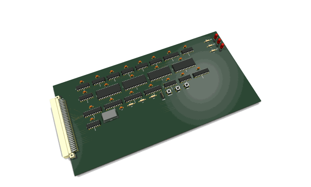
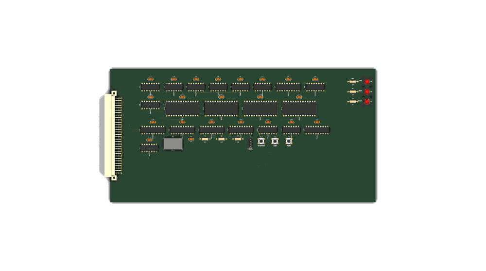
The board as routed in KiCad (3D render; top view).
Theory of operation: p8x-control-card-theory.md — deep walkthrough of inputs/outputs, signal flow, and logic.
The brain of the P8X. It generates the clock, handles reset and the front-panel run controls, holds the instruction register, and — most importantly — runs the microcode engine that drives every other card over the backplane. If a signal on the bus tells another card what to do (DOE, DLD, PSEL, ALU function, …), it originated here.
This README describes the circuit as actually built in
generators/gen_eagle.py(the canonical source). For the architectural overview see p8x-system-design.md §3; for bus pin assignments see p8x-bus-definition.md.
Chip inventory¶
| Ref | Device | Role |
|---|---|---|
| U1 | 74161 | Clock divider (÷1/2/4/8 tap via JP1) |
| U2 | 74HCT14 | Schmitt inverters — reset & switch debounce |
| U3 | 7474 | Dual D flip-flop — run/step synchronizer |
| U4 | 74HCT00 | NAND glue |
| U5 | 74HCT08 | AND glue (clock gating) |
| U6 | 74HCT32 | OR glue |
| U7 | 74377 | Instruction register (8-bit, load-enabled) |
| U8 | 74138 | DLD decoder → generates the IR-load strobe |
| U9 | 74151 | Condition multiplexer (selects 1 of 8 condition sources) |
| U10–U13 | 28C64 | Microcode ROM, 4 × 8 bits = the 32-bit control word |
| U14–U17 | 74374 | Pipeline register (latches the control word on CLK̄) |
| U18 | 74161 | Microcode step counter |
| X1 | 4 MHz osc | Master clock source |
How it works¶
Clock generation¶
The 4 MHz oscillator (X1) feeds the 74161 divider (U1). Jumper JP1 selects the raw oscillator or a ÷2/÷4/÷8 tap, so you can slow the machine down for debugging. The selected clock is gated (U5/U6) by the run/halt logic and then split into CLK and its inverse CLK̄ (via U2), both broadcast on the backplane. CLK clocks the working registers; CLK̄ clocks the pipeline latch a half-cycle earlier so the control word is already stable when CLK arrives.
Reset¶
A pushbutton + RC network feeds two 74HCT14 Schmitt inverters (U2) to produce a clean, debounced -RES. Reset clears the step counter (U18) and the instruction register (U7), and is broadcast on the backplane so every card returns to a known state (notably the Register Bank zeroes P0 → execution starts at $0000).
Front-panel run control¶
- RUN/HALT toggle and a debounced STEP pushbutton feed a 7474 (U3) synchronizer. Clocking the request through a flip-flop guarantees the machine always stops on a microcycle boundary, never mid-cycle.
- The microcode HALT bit ORs into the same stop logic (U6), so software can halt the clock; only the front panel can restart it.
The microcode engine — the core loop¶
- The instruction register (U7, a 74377) holds the current opcode. It loads
from the data bus when the DLD field = 6, decoded by U8 (74138) into the
-IRLDstrobe. - The microcode ROM address is assembled as
IR | step<<8 | cond<<12: - opcode (8 bits) from U7,
- step number (4 bits) from the U18 step counter,
- one selected condition bit from U9 (74151), chosen by the FCOND field.
- Four 28C64 EPROMs (U10–U13) output the 32-bit control word at that address.
- The 4 × 74374 pipeline latch (U14–U17) registers all 32 bits on CLK̄, so glitchy ROM transitions never reach the backplane. The latched outputs are the bus control signals: DOE0–3, DLD0–3, PSEL0–1, PINC, PDEC, ALUS0–3, ALUM, CIN, SH0–1, LDF, FCOND0–2, plus µRESET and HALT.
- The step counter (U18) increments each cycle. The µRESET bit reloads it to zero, ending the current instruction and forcing the shared fetch cycle next.
Condition multiplexer¶
U9 (74151) selects one of the flag/condition inputs (FC, FZ, FN, FV, hard 0/1, …) based on the FCOND field, and feeds it into ROM address bit 12. This is how a single opcode can branch to two different microcode paths (taken vs not-taken) without any extra sequencing logic — the condition literally selects a different ROM page.
Control word layout (32 bits)¶
See p8x-system-design.md §3.2 for the full bit map, and
microcode/genucode.py w() for the authoritative packing. In brief: bits 0–3
DOE, 4–7 DLD, 8–10 PSEL (3-bit: P0–P3 + PT scratch), 11 PINC, 12 PDEC, 13–16 ALU
S0–3, 17 ALU M, 18 CIN, 19–20 SH0/1, 21 LDF, 22–24 FCOND, 25 µRESET, 26 HALT,
27 LDZN, 28 SHCIN, 29 SETC, 30 CLRC, 31 BSEL.
LEDs¶
PWR (green), RUN (green), HALT (red) — driven from the run/halt state.