I/O Card¶
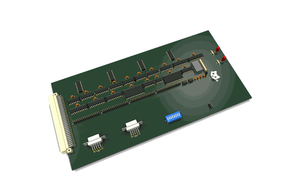
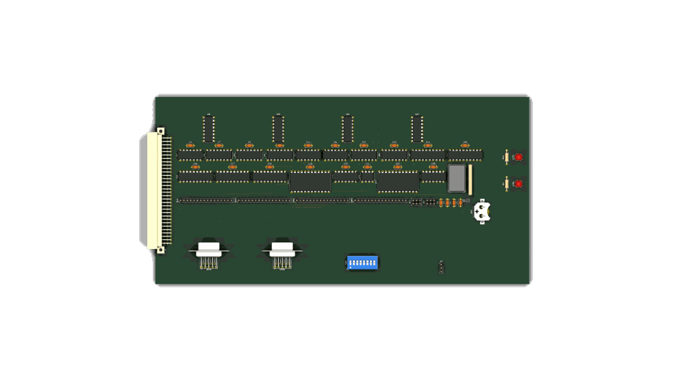
The board as routed in KiCad (3D render; top view).
Theory of operation: p8x-io-card-theory.md — deep walkthrough of inputs/outputs, signal flow, and logic.
All memory-mapped I/O lives here: an 8-switch input port, an 8-LED output port, two RS-232 serial channels via 6850 ACIAs (rev B), and a passive bus-monitor LED display that turns the machine into an Altair-style "watch it think" front panel.
Rev B (2026-09-19) — the routed KiCad board in
kicad/(not yet fabricated) adds a second 6850 (U17, ACIA2 at$FF08/09, the Kermit / serial-terminal port) on the MAX232's second channel, with its E-gate inverter in U18 (74HCT14). Each channel has its own DB9 socket and a 2×3 jumper block that swaps RX/TX (straight or null-modem). A DS1302 real-time clock (U16) is provisioned but not fitted (DNP): it is a bit-banged 3-wire part on header J3, not memory-mapped. The text below describes the rev A circuit, which rev B keeps.
| Address | Port |
|---|---|
$FF00 |
Switch input — 8 toggle switches → data bus on read |
$FF02 |
LED output — 74374 latch → 8 LEDs on write |
$FF04 |
6850 ACIA control/status |
$FF05 |
6850 ACIA data (RS-232 TX/RX) |
$FF08 |
ACIA2 control/status (rev B) |
$FF09 |
ACIA2 data (rev B) |
This README describes the circuit as actually built in
generators/gen_eagle.py. See p8x-system-design.md §7 for the overview and p8x-bus-definition.md for bus pins.
Chip inventory¶
| Ref | Device | Role |
|---|---|---|
| U1 | 7430 | 8-input NAND — I/O page ($FFxx) detector |
| U2 | 74138 | Port decoder (A1–A3 → up to 8 port selects) |
| U3 | 74138 | DOE decoder (read enable) |
| U4 | 74138 | DLD decoder (write strobe) |
| U5 | 74HCT32 | OR glue (read/write strobe gating) |
| U6 | 74HCT08 | AND glue (ACIA enable) |
| U7 | 74161 | Baud-rate divider |
| U8 | MAX232 | RS-232 level shifter (the one non-TTL part) |
| U9 | 74244 | Switch-input buffer |
| U10 | 74374 | LED output latch |
| U11–U13 | 74244 | Bus monitors — A0–7, A8–15, D0–7 |
| U14 | 6850 | ACIA (asynchronous serial) |
| U15 | 74HCT00 | NAND glue |
| U16 | DS1302 | Real-time clock, DNP (rev B; 3-wire on J3, not memory-mapped) |
| U17 | 6850 | ACIA2 at $FF08/09 (rev B) |
| U18 | 74HCT14 | Inverter — ACIA2 enable gate (rev B) |
| X2 | 2.4576 MHz osc | Baud clock source |
How it works¶
Port decoding¶
U1 (7430) detects the $FFxx page exactly as on the memory card. Within the page,
U2 (74138) decodes the low address lines into individual port selects (-P0, -P1,
-P2, …). Read vs write comes from the DOE decoder (U3 → -RD) and DLD decoder
(U4 → -MEMW), gated in U5/U6 into per-port read/write strobes.
Switch input ($FF00)¶
Eight toggle switches with a SIP pull-up network feed a 74244 (U9). On a read of
$FF00, U9 is enabled and drives the switch states onto D0–D7.
LED output ($FF02)¶
On a write to $FF02, the 74374 (U10) latches D0–D7. Its outputs drive an LED bank
through series-resistor networks, so the port value is visible at a glance.
Serial (6850 ACIA, $FF04–$FF05)¶
The 6850 ACIA (U14) handles asynchronous serial. Its enable is the $FF04/05
port select gated with the clock (U6/U15) for correct E-clock timing. A 74161
(U7) divides the dedicated 2.4576 MHz oscillator (X2) by 16 to make the
TX/RX baud clock. The MAX232 (U8) — the one concession to non-TTL parts —
converts the ACIA's TTL levels to/from RS-232 ±voltages on the serial header,
using its four external charge-pump capacitors.
Bus-monitor display (passive)¶
Three 74244 buffers (U11/U12/U13) permanently sample A0–7, A8–15, and D0–7 and drive three LED banks. They cost nothing logically — no decode, no bus access — but combined with the control card's single-step button they let you literally watch the address and data buses change one microcycle at a time.
Bus codes this card owns¶
- DOE: 7 = read (the active port drives D0–D7) — shared decode convention with memory
- DLD: 7 = write (
MEMW) — the active port latches D0–D7
LEDs¶
PWR (green), IOSEL (yellow — an I/O port is selected), plus the LED output port and the 24-bit bus-monitor banks.