CF-IDE Card
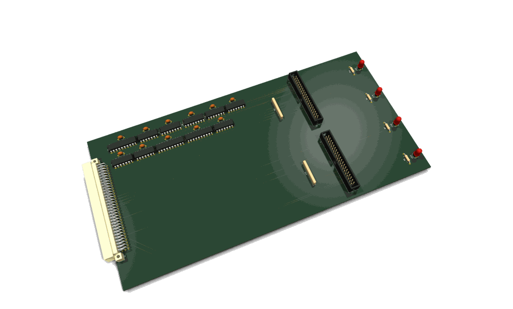
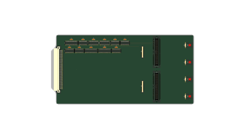
The board as routed in KiCad (3D render; top view).
Theory of operation: p8x-cf-card-theory.md — deep walkthrough of inputs/outputs, signal flow, and logic.
Adds mass storage: a CompactFlash card running in 8-bit True IDE mode, memory-mapped into the I/O page at $FF10–$FF17. This is what lets the P8X load an OS and a filesystem from removable media instead of living entirely in ROM.
Rev B (2026-09-19): two drives. The routed KiCad board in
kicad/(not yet fabricated) carries a second, fully decoded CF drive: drive 0 at$FF10–$FF17on header J2, drive 1 at$FF18–$FF1Fon header J5, each with its own 74245 buffer, strobe glue, pull-ups and activity LED (master/slave on one channel was rejected as unreliable for True IDE CF). Software follow-up: the firmware CF driver and the emulator select drive 1 with the device bit on$FF10–$FF17, so drive 1 on this card needs a drive-selectable port base first; drive 0 works unchanged. The chip-by-chip text below describes the drive-0 circuit.This README describes the circuit as actually built in
generators/gen_eagle.py. For the storage software stack see p8x-cf-os-design.md and p8xfs-v2-hierarchical.md; for bus pins see p8x-bus-definition.md.
Chip inventory
| Ref | Device | Role |
|---|---|---|
| U1 | 74245 | Bidirectional data-bus transceiver (P8X bus ↔ CF data) |
| U2 | 7430 | 8-input NAND — I/O page ($FFxx) detector |
| U3 | 74138 | DOE decoder (read enable) |
| U4 | 74138 | DLD decoder (write strobe) |
| U5 | 74HCT14 | Schmitt inverters — strobe/select conditioning |
| U6, U7 | 7410 | 3-input NAND — register/select decode and -IOR/-IOW gating |
| U8 | 74HCT08 | AND glue — chip-select combine, activity LED |
| J2 | 40-pin IDE | CompactFlash / IDE connector |
How it works
Address decode ($FF10–$FF17)
U2 (7430) detects the $FFxx page. The CF task-file registers occupy
$FF10–$FF17; the low address lines A0–A4 select the individual IDE register, and
the 7410 NANDs (U6/U7) combine the page hit with A3/A4 to produce the two True-IDE
chip selects -CS0 (command block) and -CS1 (control block). U8 ANDs them
into a single -CFSEL "this card is addressed" signal.
Read / write strobes
DOE code 7 (-RD) and DLD code 7 (-MEMW) are decoded by U3/U4. Gated with the
clock and -CFSEL through U5/U7, they become the IDE bus strobes -IOR (I/O
read) and -IOW (I/O write) on the connector. These are the standard True-IDE
timing signals the CF card expects.
Data path
A single 74245 (U1) bridges the P8X data bus and the CF data lines (the low 8
bits — this is 8-bit mode, so the high byte of the IDE 16-bit data path is unused).
Its direction follows -IOR (read = drive toward the P8X bus) and it is
enabled only when the card is selected (-CFOE), so it never contends with
other bus drivers.
Status lines
The CF's open-drain status lines — IORDY, -PDIAG, -DASP — are pulled up
through a SIP resistor network (RN1). -DASP (drive active / slave present) also
drives the activity LED.
Reset
The backplane -RES is wired to the IDE connector's reset pin, so the CF card is reset together with the rest of the machine.
Bus codes this card owns
- DOE: 7 = read (drives D0–D7 when
$FF10–$FF17is addressed) - DLD: 7 = write (
MEMW) — shared decode convention with memory & I/O cards
The CF card, memory card, and I/O card all decode the same DOE=7 / DLD=7 codes; the address decode (which page/region) is what keeps exactly one of them active per cycle.
LEDs
PWR (green), ACT (yellow — card selected / access in progress), DASP (green — CF present and active).