P8X Bus Test Card — Design¶
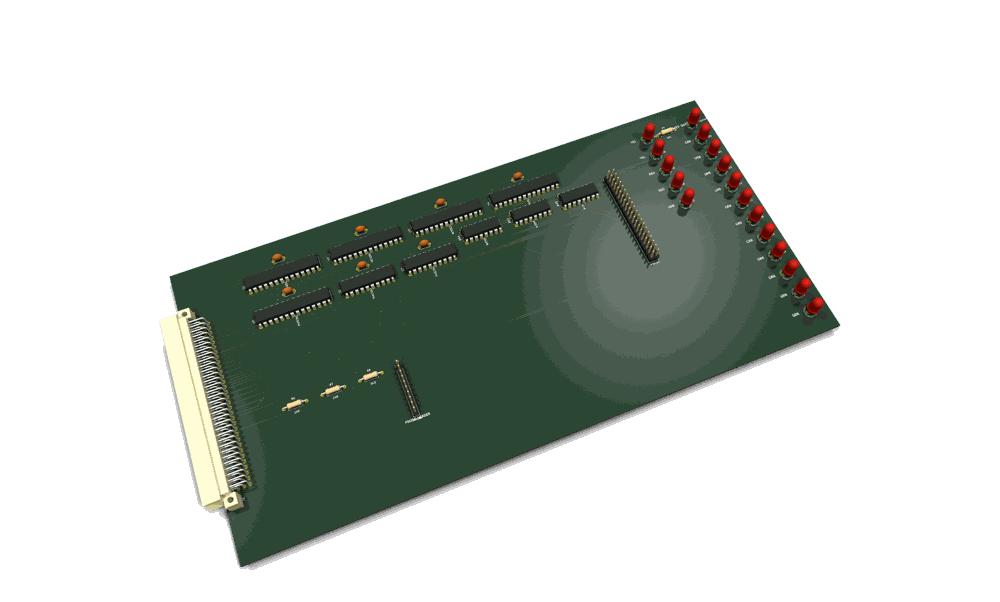
The board as routed in KiCad (3D render; top view).
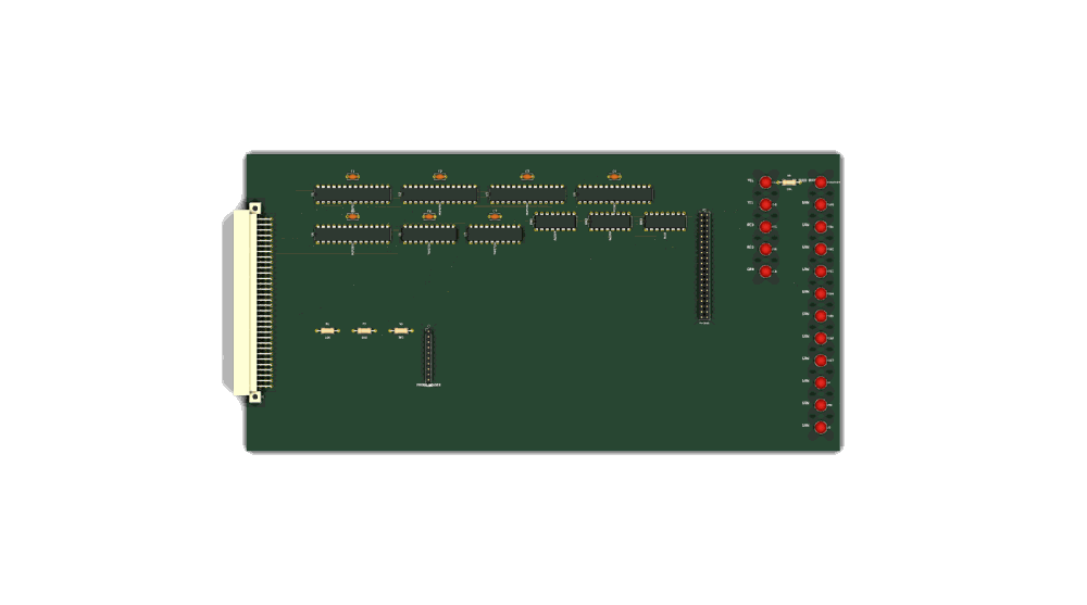
Status: designed and routed in KiCad, not fabricated. The board is in
kicad/(280 × 140 mm, 4-layer, 0 unconnected, Gerbers + renders), built from the samegen_eaglenetlist as the rest of the machine. Nothing here has been fabbed or verified against real silicon. Numbers are calculated, not measured. Open items are listed in §10; the firmware (firmware/buscon.c) has not been compiled yet (seeBACKLOG.md).
A USB-attached card that brings up the rest of the machine, one card at a time, by driving the backplane directly and diffing what it sees against the emulator.
1. The thesis: this is a control card you can type at¶
The P8X backplane does not carry a conventional address/data bus with RD/WR.
It carries the horizontal microcode control word. DOE selects which card
drives D0–D7; DLD selects which latches it; PSEL selects which pointer drives
A0–A15; ALUS/ALUM/CIN/BSEL/SH*/LDF/LDZN/SETC/CLRC are control-store outputs
wired straight to the cards. Those lines are driven by the control card's pipeline
register (U14–U17, 74374) — nothing else drives them.
So the useful tool is not a bus pirate. It is a card that sits exactly where the control card's pipeline output sits and presents the same word, one microcycle at a time, under your fingers.
That framing is what makes card-level bring-up possible: each card can be exercised with the rest of the machine absent.
- Memory card alone.
A0–A15is input-only to every card except the register bank (§3.2 of the bus definition). With the reg-bank out, the address bus is ours: drive an address,DOE=MEM, step, readD. - ALU card alone. Drive
ALUS/ALUM/CIN/BSEL, read the result andFC/FZ/FN/FV. No PC, no memory, no microcode. - Reg-bank alone.
PSEL+PTRL/PTRH+PINC/PDEC, watchA0–A15.
1.1 The card is the sequencer¶
The microword has 19 fields (microcode/genucode.py, w()), but only 16 reach
the backplane. Three are the control card's own business:
| Field | Why it never leaves the control card |
|---|---|
fcond |
selects which flag the sequencer branches on |
urst |
resets the microstep counter to 0 |
halt |
stops the clock |
So the bus test card drives the 16 bus-visible fields and is itself the sequencer for the other three — "what word comes next" is just the next line of the test script. It never models the microcode ROM, the step counter, or the pipeline. It only has to reproduce the phasing (§4).
1.2 The emulator is the reference model¶
emulator/p8xemu.c already models every line this card touches — the BSEL
B-input mux, V-flag derivation, the DOE/DLD decode. So the same ASCII script
can drive the emulator and the card, and the two outputs diffed.
That is the pattern this project already uses everywhere else: p8cc.py vs
p8cc.c as a differential oracle, and the byte-identical C/asm command twins.
Bring-up becomes "run the tests against real silicon and diff" rather than
"poke it and squint at a scope".
2. Scope¶
| Function | Drive/read all 59 backplane signals + 8 high-Z probes, over USB, in ASCII |
| Timing | Static/stepped only. Not a logic analyser. |
| Bus role | Drives when the owning card is out; listens otherwise |
| Host link | USB CDC, line-oriented ASCII (typable by a human, parseable by a script) |
| Board | 280 × 140 mm, 4-layer, as routed in KiCad (first designed as a 160 × 100 mm Eurocard, W=160, H=100), DIN 41612 96-pin, MABC96R |
| Firmware | C, Pico SDK |
Static-only is the load-bearing decision. It is what allows SPI port expanders instead of an FPGA, and — more importantly — what makes the series resistors in §3.2 free. Every safety property below follows from it.
3. Bus ownership and safety¶
3.1 Wake state: drive nothing¶
Every pin comes up as an input. The card drives nothing until a test claims it. There is no presence strap and no hardware interlock: a test asserts which cards are absent, and that assertion is a line in the script.
This works because contention is made non-destructive, not impossible (§3.2).
The idle state falls out of the bus's own encoding: all-zeros is inert.
DOE=0 is bus-idle, DLD=0 is no-load, PINC/PDEC/LDF=0 are no-ops — and -RES
is active-low, so low means held in reset.
There are no bus pull-downs on this card (an earlier draft had six; they were
cut — see §3.1a). A floating word is only dangerous when a clock edge can latch
it, so the one line worth conditioning is the clock, and firmware does it: the
Pico drives CLK/CLKB low as its first action after reset (bus_init() in
buscon.c), before accepting any command. From that point nothing downstream can
latch a floating word. Everything else stays Hi-Z until a drive command claims
it.
CLK held low is the real interlock. With no rising edge, nothing latches
anywhere, whatever else is on the bus.
3.1a Why no pull-downs — the scenario they defended does not need them¶
Pull-downs would only matter in one state: this card Hi-Z (not driving) and the control card absent, so nothing drives the ~40 control lines. That state:
- only exists during bring-up — the real machine always has the control card driving these lines; "control card absent" is created solely by this workflow;
- is a brief power-on transient — you power up, then your first command claims a group and drives it;
- has a recoverable worst case — floating
DOEis one-hot decoded, so it enables one wrong source ontoD0–7(no contention); floatingDLD+ a glitching float onCLKcould fire one spurious SRAM write. On a bench tool that is a byte you rewrite, not a dead chip.
Spending three resistor networks — the bulk of the board's passives — so a bench instrument can condition other cards' floating inputs during a transient the real machine never has is the wrong place to solve it. The only line with teeth (the clock) is handled in firmware (§3.1). The unguarded window shrinks to power-on-to-firmware (~tens of ms), closed by bringing the backplane up before/with USB.
3.2 The 1 kΩ probe series, and the contention tradeoff¶
The bus lines carry no series resistors. The MCP23S17 runs at VDD = 5 V, so its GPIO is native 5 V against the all-74HCT machine (24 HCT parts in the BOM, no LSTTL) — no level translation is needed, which is why the earlier 1 kΩ bus networks were dropped. Consequence, stated plainly:
- Driving an HCT input (CMOS, ~1 µA) gives a full-rail ~5 V — better than the old 4.55 V through a series R.
- Contention — a test asserting
driveon a group whose card is actually present — is now limited only by the two parts' own Ron, roughly 25–50 mA. That is within both the MCP's and the 74HCT's per-pin abs-max, so it survives a brief mistake, but it is not "safe indefinitely." Thedriveassertion therefore carries real weight; hold contention and you can cook a pin. (This is the one place the board traded safety margin for parts — see §10; if it proves too sharp, 100 Ω bus series would cap contention at ~5 mA for the cost of the networks back.)
The 8 probe lines keep 1 kΩ (RN3, DIP-16 network), because a slipped grabber is
over-voltage the operator cannot design away: a grabber onto 12 V gives
(12−5)/1k = 7 mA into the MCP's internal ESD clamp, under its 20 mA rating — so
no external clamp diodes are needed.
3.3 Passive allocation — do not double up¶
A pull-up and a pull-down on the same line sit at mid-rail and leave every HCT input indeterminate. After the pull-down cut, the only passives on the bus are the backplane's, plus this card's probe series:
| Line | Passive | Where |
|---|---|---|
D0–D7 |
10k pull-up (RN1, exists) | backplane |
-IRQ |
10k pull-up (R4, added) |
backplane |
-RES |
none | — (control card drives it push-pull; see below) |
A0–A15, control, CLK/CLKB |
none | — (firmware holds the clocks; §3.1) |
| Probes | 1k series | this card (RN3, DIP-16 network) |
This card puts no passive on D, -RES, or -IRQ — those belong to the
backplane.
-IRQ needs its pull-up; -RES does not. -IRQ is wired-OR (open-drain), so
the 10k is its only high state — added on the backplane as R4 (one resistor,
all slots, always present). -RES is driven push-pull by the control card's
74HCT14 (with a power-on RC), so there is nothing to pull against — a resistor
there would be a weak load the gate overrides. An earlier draft listed a "new 10k
pull-up on -RES"; that was wrong on both counts (unnecessary, and if anything the
fail-safe polarity is a pull-down, since float-low = reset asserted). The only
unguarded -RES moment is control-card-absent bring-up — and this card drives
-RES then, so even that is covered.
3.4 Presence detection is functional, not electrical¶
When a test wants to verify its assumption before claiming lines, it can — with no straps and no card modifications:
- Control card:
CLK/CLKBare complements by definition. Enable the MCP's internal pull-ups on both, release, and read: a driving control card overrides the weak (~100 kΩ) pull-ups to give01/10; an absent one lets both float to the pull-up rail =11. (With the old pull-downs this read00; the logic is the same, the resting value differs.) Still guaranteed, unlike level-probing — a halted control card and an absent one look identical if you only watch for edges. - Reg-bank: pulse
PINCand see whetherA0–A15changes. - ALU: drive an operation and see whether the flags respond.
4. Clock discipline — the part that is easy to get wrong¶
4.1 The machine is fully static¶
62256 SRAM + 28C64 EEPROM. No DRAM, no refresh, no monostables, no 555s. The control card already has a single-STEP button, so stepping is a designed-in capability. The clock can be parked in any phase indefinitely.
4.2 CLKB is not decorative¶
-MEMW (memory card, U8), and both CF strobes (-IORD/-IOWR), are gated
combinationally by CLK̄. The I/O and LED cards clock their latches from it.
Drive CLK alone and writes never strobe — which presents as a dead memory
card and sends you scope-probing a fault that does not exist. Both lines are
driven independently.
4.3 The four states, and why "both low" matters¶
CLK |
CLKB |
State |
|---|---|---|
| 0 | 0 | rest/setup — no edge, every strobe gated off |
| 0 | 1 | phase A — strobes assert, source drives D, everything settles. Sample D here. |
| 1 | 0 | phase B — destination register latches; strobes deassert, so an SRAM write commits on this transition |
| 1 | 1 | illegal — strobes enabled with CLK already high. Reachable deliberately, for fault injection. Never in a normal step. |
step = rest → A → B → rest.
rest (both low) is a state the real machine physically cannot produce — its
CLKB is always ¬CLK. It exists here because it is load-bearing twice over:
- The microword is not atomic. Five expanders update sequentially over SPI, and
the address bits live on a different chip from
DLD. SettingDLD=MEMWwhileCLKBis high asserts-MEMWimmediately, while address bytes are still arriving — strobing writes into whatever addresses flicker past. Parking at00gates every strobe off while the word settles. - Gated clocks. The ALU's flag register (U17) is clocked by
CLK & (LDF | LDZN)through U31. RaiseLDFwhileCLKis already high and that AND gate goes 0→1 — a manufactured rising edge, latching phantom flags. The real machine cannot do this: its pipeline latches onCLK̄, so the control word only ever changes asCLKfalls. This card reproduces that discipline by always returning toCLK=0 before the word changes.
Rule: the microword may only change while CLK is low. rest enforces it.
5. Circuit¶
5.0 Block diagram¶
Signal flow is top-to-bottom: host → Pico → SPI → expanders → series resistors → backplane. LEDs hang off the bus side; the probe header hangs off U5.
   host (Mac) ═══ USB ═══╗                                  8 STATUS LEDs
   ASCII protocol        ║                          5V-OK ARMED LISTEN CLK
   (line-oriented)       ║                          CLKB -RES ERR USB-ACT
                         ▼                                   ▲
                  ┌──────────────────────────────────────────┴──┐
                  │ A1   Pico / RP2040   (C firmware, USB CDC)   │
                  └──┬───────────────────────────────────────▲───┘
        SCK SI CS RESET │ 3.3V                          5V │ SO
                        ▼                                  │
              ┌─────────────────────┐          ┌───────────┴────────┐
              │ U6  74HCT244  @5V   │          │ 2-resistor divider │
              │ 3.3V in → 5V out    │          │ 5V → 3.3V          │
              │ (HCT VIH = 2.0 V)   │          └────────────────────┘
              └─────────┬───────────┘   one chip, ONE direction: the Pico only
                        │ SPI @5V       SENDS to the expanders. No '245 needed.
                        ▼
  ┌────────────────────────────────────────────────────────────────────────┐
  │ U1..U5   5 × MCP23S17 @5V   —  80 lines, per-pin direction + pull-ups   │
  │   U1   GPA = D0-7                    GPB = A0-7                        │
  │   U2   GPA = A8-15                   GPB = DOE0-3, DLD0-3              │
  │   U3   GPA = PSEL0-2 PINC PDEC       GPB = ALUS0-3, ALUM, CIN,         │
  │              CLK CLKB -RES                 SH0, SH1                    │
  │   U4   GPA = LDF LDZN SETC CLRC      GPB = FC FZ FN FV  (read-only)    │
  │              BSEL SHCIN -IRQ               + 4 spare                   │
  │   U5   GPA = PR0-7  (probes, high-Z) GPB = SPARE12-19                  │
  └───────┬──────────────────────────────────────────────────┬─────────────┘
          │                                                  │
          │  NO bus series R: MCP@5V is native 5V (no level        │ 1k (R25-32)
          │  shift needed). Trade: contention limited only by        ▼
          │  device Ron (~25-50mA, abs-max-safe, not indefinite)  ┌──────────────┐
          │  → the `drive` assertion carries weight.              │ J2  2×5 hdr  │
          │                                                       │ 8 probes     │
          ├──────────────► U7  74HCT244 ───────┐   probe 1k for   │ + 2 GND      │
          │                probe LED buffer    │   over-V only    └──────┬───────┘
          │                (~1 µA bus load)    ▼   (slipped grabber)  ribbon→grabbers
          │                            16 LEDs: PR0-7 + 8 status
          │   (D0-7 / A0-15 monitor arrays CUT — redundant w/ ASCII readback; §5.4)
          │
          │   NO bus pull-downs: firmware drives CLK/CLKB low on boot (the only
          │   line a floating word can latch through); everything else Hi-Z until
          │   a `drive` claims it. See §3.1/§3.1a.
          ▼
  ┌────────────────────────────────────────────────────────────────────────┐
  │ J1   DIN 41612 96-pin (MABC96R)   →   P8X BACKPLANE                    │
  │   D0-7   A0-15   ~40 control   CLK/CLKB   -RES   -IRQ   FC/FZ/FN/FV    │
  └────────────────────────────────────────────────────────────────────────┘
     backplane owns these passives, NOT this card (never double up — a pull-up
     and a pull-down on one line sit at mid-rail):
       RN1   10k pull-UP on D0-7   (exists)
       R4  10k pull-UP on -IRQ   (added; wired-OR needs it, see §7)
       -RES  NO pull — control card drives it push-pull (§3.3)

  POWER   backplane +5V ─┬─────────────────────► U1..U10  @5V
                         ├──►|◄── Schottky ────► Pico VSYS (pin 39)
                         │   (lets USB + external coexist; the Pico's own
                         │    VBUS diode blocks backfeed into the host)
                         └─── 2-R divider ─────► Pico GPIO — 5V SENSE.
                              Firmware refuses to drive without it: USB-on /
                              backplane-off would otherwise leave the Pico
                              driving unpowered expander inputs (latch-up).
5.1 Pin budget¶
| Group | Lines | Notes |
|---|---|---|
D0–D7 |
8 | bidirectional |
A0–A15 |
16 | driven only when the reg-bank is out |
| Control | 31 | DOE×4, DLD×4, PSEL×3, PINC, PDEC, CLK, CLKB, LDF, LDZN, SETC, CLRC, BSEL, ALUS×4, ALUM, CIN, SH0, SH1, SHCIN, -RES, -IRQ |
| Flags | 4 | FC/FZ/FN/FV — read-only (ALU card drives them) |
| 59 | = the backplane signal count in §2 | |
| Probes | 8 | high-Z in |
| Total | 67 |
5 × MCP23S17 = 80 lines with per-pin direction and per-pin pull-ups, so 13
spare. Eight of those are wired to SPARE12–19 (already routed slot-to-slot, so
they cost nothing now and need no backplane re-spin later); five are left free.
Per-chip allocation is in the block diagram above.
5.2 Parts¶
| Ref | Device | Role | New to generator? |
|---|---|---|---|
| U1–U5 | MCP23S17 (DIP-28) | 80 bidirectional 5 V lines, SPI | add |
| U6 | 74HCT244 | SPI level-shift, 3.3 V → 5 V (SCK/MOSI/CS/RESET) | reuse |
| U7 | 74HCT244 | probe LED buffer | reuse |
| A1 | Pico (2×20 headers) | RP2040, USB CDC | add |
| J2 | 2×5 header | 8 probes + 2 GND | add |
| RN1 | RNISO8D (DIP-16) | probe-LED current-limit, 8×330 Ω isolated | add |
| RN2 | RNISO8D (DIP-16) | status-LED current-limit, 8×330 Ω isolated | add |
| RN3 | RNISO8D (DIP-16) | probe series, 8×1 kΩ isolated | add |
| R5–R8 | RES | 5V-sense divider (×2), MISO divider (×2) | reuse |
| LED1–8 | LED (through-hole) | probe activity, 8 individual LEDs | reuse |
| LED9–16 | LED (through-hole) | status, 8 individual labelled LEDs | reuse |
| J1 | MABC96R | DIN 41612 edge connector | supplied by card() |
card() also supplies the per-IC 100 nF decoupling caps, so the project's caps
rule is satisfied structurally rather than by remembering.
Level shifting is one chip, one direction. A bidirectional 74HCT245 is not
needed: the Pico only sends to the expanders (SCK/MOSI/CS/RESET). HCT's
VIH=2.0 V accepts 3.3 V and its outputs swing to 5 V. MISO returns
through a two-resistor divider. The MCP23S17s run at 5 V and talk TTL directly.
5.3 Power¶
All from backplane +5 V (per-slot budget is not a constraint here).
- Expanders + buffers: backplane 5 V directly.
- Pico: backplane 5 V → Schottky → VSYS. This is the documented way to let an external supply and USB coexist; the Pico's own VBUS diode blocks backfeed into the host.
- 5 V sense: a divider from backplane +5 V to a GPIO. Firmware refuses to drive without it. This closes the one bad case: USB plugged in with the backplane off leaves the Pico alive driving unpowered expander/buffer inputs — latch-up territory. Two resistors.
Worst case ≈ 250 mA (16 LEDs ≈ 65 mA, Pico 30–100 mA, five expanders, 2 buffers).
5.4 LEDs¶
16 individual through-hole LEDs, each silkscreen-labelled (LED1–8 probes,
LED9–16 status) — replacing the two DIP-16 bar arrays. They still cost zero
expander pins: the probe display taps the bus side through a 74244 buffer
(io-card monitor pattern, U11–U13), loading the line with ~1 µA, and the status
LEDs run straight off Pico GPIO (ST0–7 = GP7–GP14).
Silk labels are abbreviated (≤3 letters + a digit) to fit beside the LED5s.
| Ref | Silk | Meaning | Source |
|---|---|---|---|
| LED1–8 | PRB0–PRB7 | probe 0–7 activity | 74244 buffer (U7) |
| LED9 | 5V | 5 V present | Pico GP7 |
| LED10 | ARM | armed (driving) | Pico GP8 |
| LED11 | LIS | listen mode | Pico GP9 |
| LED12 | CLK | clock | Pico GP10 |
| LED13 | CKB | clock-bar (CLKB) | Pico GP11 |
| LED14 | RES | -RES asserted | Pico GP12 |
| LED15 | ERR | error | Pico GP13 |
| LED16 | USB | USB activity | Pico GP14 |
Individual parts cost more board space and 14 extra placements than the arrays,
but every indicator gets a printed name next to it — worth it on a bench tool you
read by glancing. The silkscreen VALUE is the (abbreviated) function (PRB0, 5V,
RES, …), not the LED color, so the board reads as meaning rather than parts.
Colors (probes green; status green/yellow/red by severity) are provisional — tied
to the §10 open item on the status set — and ride along as the schematic label.
The D0–7 and A0–15 monitor arrays were cut. They were redundant with the ASCII
readback while stepping (the card reads the bus back over SPI and prints it
exactly), and only an activity blur when the machine free-runs faster than SPI can
sample. Removing all three took 3 × 74244 + 3 × RNISO8 + 3 × LEDARR8 off the
board (10 ICs → 7). The two kept arrays each show something not otherwise visible:
the probe display is the point of the probe feature, and status is card state.
If you want the bus monitor back, it re-adds cleanly — the _ledbuf() helper and
the io-card precedent are still there.
5.5 Board¶
Superseded by the KiCad flow (2026-09-18). Every plug-in card, this one included, is now a uniform 280 × 140 mm 4-layer board with the bus connector on the left edge (KICAD-BOARDS.md); the routed board has its LED bank on the right edge. The 160 × 100 mm reasoning below is the Eagle-era design record.
160 × 100 mm — a standard Eurocard, same as every other card.
This card was originally scoped at W=200 on the assumption it needed the extra
40 mm for the USB socket, probe header and LED bank. That was decided at ~45
parts. Three rounds of cuts (the bus pull-down networks, the D0-7/A0-15 monitor
LED arrays, the bus series resistors) took it to 27, and at 27 the extra width is
no longer earning its place: auto-placement fits everything in two rows using
31 % of the board area, with the last part ending at x=150 — 10 mm of slack
against the 160 mm edge.
Reverting to the standard size is worth more than the space it costs:
- Mechanical. 200 mm cantilevered off the DIN connector, carried by just the two mounting holes at y=±45, was the real problem. This card gets handled far more than the others — every grabber clip and every USB insertion put a moment through the connector. At 160 mm it sits in the card guides like everything else, and the outer-standoff/guide-rail question disappears.
- Fabrication. One panel size, one guide spacing, one mechanical drawing across the whole set.
J1 still hugs the left edge (x≈0) with parts flowing left-to-right, so the USB socket, the 2×5 probe header and the LED bank remain at the outer end — the end you can reach with the card seated. That property came from the flow direction, not from the extra width, so nothing is lost by dropping it.
Auto-flow placement, as a fit check only (the parts ship parked off-board
in p8x-bustest-card.brd, to be placed from the ratsnest):
| row | contents | x extent |
|---|---|---|
| edge | J1 | 1.7 → 14.2 |
| 1 | U1–U7 + their decoupling caps, A1 (Pico) | 17.1 → 150.0 |
| 2–3 | J2, D1, R5–R8, RN1–RN3, LED1–16 | wraps to ~3 rows |
0 parts overflowing the outline, 0 footprint overlaps. This is auto-flow output, not a considered layout — it proves the card fits, and is a starting point for hand placement, not the final arrangement.
6. The ASCII protocol¶
Field names are genucode.py's names, verbatim — that is what makes a script
meaningful against both the card and the emulator.
DOE  = idle A B T T2 ALU FLAGS MEM PTRL PTRH        (0..9)
DLD  = none A B T T2 FLAGS IR MEMW PTRL PTRH        (0..9)
PSEL = P0 P1 P2 P3 PT PT2                           (0..5; PT/PT2 hidden scratch)
also: PINC PDEC ALUS M CIN SH0 SH1 SHCIN LDF LDZN SETC CLRC BSEL
Responses are KEY=VAL — typable and trivially parseable. Errors are !ERR
<reason>: unmistakable, the same instinct as the compiler's poison directive.
p8x> id
P8XBUS 1.0  5V=ok  owns=(none)

p8x> owns                       ; power-on: drives nothing
drive=(none)  hiz=ctrl,addr,data,probes

p8x> drive ctrl addr            ; this test asserts: control card and reg-bank are OUT
p8x> w DOE=MEM DLD=none PSEL=P0
p8x> a 2000
p8x> step                       ; rest -> A -> B -> rest
p8x> r D
D=EA
p8x> r flags
FC=0 FZ=1 FN=0 FV=0
p8x> probe
PR=1011_0010
step performs the correct phasing by default; reaching the illegal CLK=1
CLKB=1 requires an explicit clk 1 1.
7. -IRQ: fix the polarity before anything is built¶
The bus definition calls it IRQ (active-high by name) but describes it as "any
card may pull it" — that is wired-OR, which means open-drain, which means
active-low. Both cannot be true. The emulator does not settle it: it models
interrupts abstractly (a write to $FF06 sets irq_pending), never as a line.
And the circuit is the one unbuilt hardware item (control card U20/U21, DNP).
Recommendation: treat it as -IRQ, active-low, open-drain, with a 10 kΩ pull-up
on the backplane. Cards assert with an open-drain buffer — 74HC07 is a hex
open-drain buffer in DIP, so the through-hole rule holds. This is what makes "any
card may pull it" actually work: open-drain drivers cannot fight each other,
whereas the HCT push-pull parts used everywhere else in this machine physically
cannot be wire-ORed. Active-high would need open-source drivers or a diode-OR —
both worse.
Done (backplane not yet fabbed, so it cost nothing): the 10 kΩ pull-up now
exists on the backplane as R4 (end zone, beside RN1), so the wired-OR line
has its high state regardless of which cards are installed. Still open, on the
control card: the open-drain assert/sample side (U20/U21, DNP) — task #26. Note
-RES did not get a matching pull (it is push-pull driven; §3.3).
This card can then assert -IRQ on demand and single-step the machine into the
$08 vector — which is how the interrupt hardware should be brought up, with the
emulator's IE/irq_pending/$08-injection model as the reference.
8. Bring-up sequences¶
Each runs with only the card under test in the backplane.
Memory card. Drive A, DOE=MEM, step, read D. Walk all 8 K and diff
against eeprom.bin — the golden image already exists. Then write/read-back the
SRAM (DLD=MEMW; note the write commits on the A→B transition, §4.3).
ALU card. Sweep ALUS/ALUM/CIN/BSEL over operand pairs; diff result and
FC/FZ/FN/FV against the emulator. At ~40 µs/vector, all 65,536 operand pairs
for one function ≈ 3 s; all 16 functions well under a minute. This is exhaustive
verification of the card that gates the T-operand work, including the 74157 B-mux.
Reg-bank. PSEL + PTRL/PTRH load, PINC/PDEC, read A. Covers all six
pointers including the hidden PT/PT2 scratch.
Then insert the control card, release everything, and watch the real machine run in listen mode.
9. Known limitation: IR¶
IR lives on the control card, so DLD=IR is a no-op during card-level
bring-up — the only time this card drives. Instruction-register loading cannot
be exercised until the control card is in, at which point this card is
listen-only. That is inherent to the approach, not a fixable gap.
10. Open items¶
- Mating orientation — the bus definition still carries "VERIFY against physical connectors before first fab". Unresolved, and it bites this card as much as any other.
- Where
CLKparks when halted — affects listen-mode sampling only. - Status LED set — the eight in §5.4 are a guess and want a second opinion from whoever will stare at them.
- Contention margin — dropping the bus series R (§3.2) means a wrong
driveis limited only by device Ron (~25–50 mA, abs-max-safe but not indefinite). Accepted for a careful bench tool; reversible by adding 100 Ω bus series (caps at ~5 mA) if it proves too sharp in use. - Layout — done in KiCad (2026-09-18): auto-placed and Freerouting-routed on the uniform 280 × 140 mm card, 0 unconnected. (The Eagle-era note here said the 41 parts fit 160 × 100 at 31 % utilisation, with nothing placed and no copper.)
- Nothing here is measured. Every number above is calculated from datasheet values and the existing design docs.