Register Bank Card¶
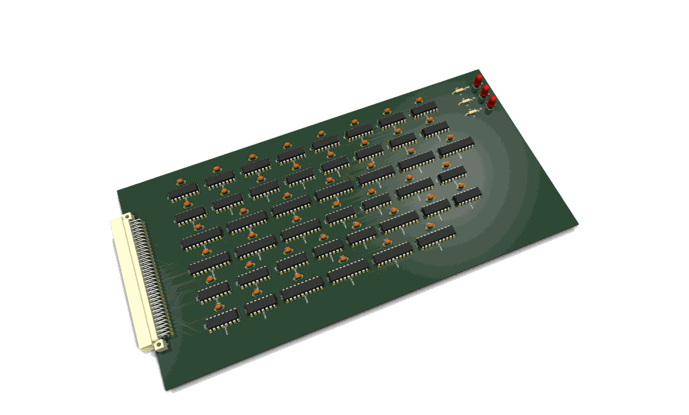
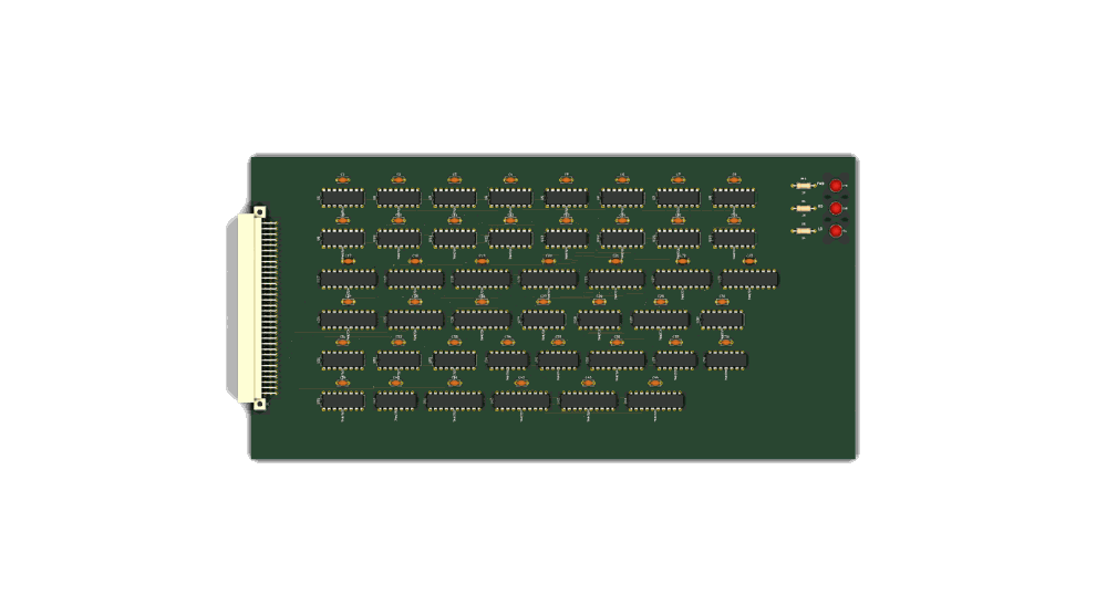
The board as routed in KiCad (3D render; top view).
Theory of operation: p8x-regbank-card-theory.md — deep walkthrough of inputs/outputs, signal flow, and logic.
The largest card and the architectural centerpiece of the P8X. It holds the four 16-bit pointer registers P0–P3 and always drives the address bus — there is no separate MAR. Every memory access is "select a pointer, drive its value on A0–A15, optionally increment/decrement at the clock edge."
| Pointer | Role |
|---|---|
| P0 | Program counter |
| P1, P2 | General pointers (indirect addressing modes) |
| P3 | Stack pointer (empty-descending) |
This README describes the circuit as actually built in
generators/gen_eagle.py. See p8x-system-design.md §4 for the architecture and p8x-bus-definition.md for bus pins.
Chip inventory¶
| Ref | Device | Role |
|---|---|---|
| U1–U16 | 74169 | The four pointers — 4 synchronous up/down counters each (16 bits) |
| U17–U24 | 74244 | Pointer-select buffers — gate the selected pointer onto the on-card pointer bus (2 per pointer) |
| U25, U26 | 74244 | Address-bus drivers — pointer bus → backplane A0–A15 (always enabled) |
| U27, U28 | 74257 | Readback byte mux — pick low or high byte of the selected pointer |
| U29 | 74244 | Readback driver — selected byte → data bus D0–D7 |
| U30 | 74138 | DLD decoder (load low / load high) |
| U31 | 74138 | DOE decoder (read low / read high) |
| U32 | 74139 | Load decoder — which pointer's byte gets loaded |
| U33 | 74139 | Select + count decoder — which pointer drives address / counts |
| U34 | 7402 | NOR — count-request gating |
| U35 | 74HCT14 | Inverters — up/down direction and select polarity |
| U36 | 74244 | Forced-zero buffer for the P0 reset trick |
| U37, U38 | 74HCT08 | AND glue — reset-gated P0 loads, LED drive |
How it works¶
The pointers (74169 cascade)¶
Each pointer is four 74169 synchronous up/down counters, 4 bits apiece. They
are cascaded for full 16-bit carry/borrow: the master count enable (-CNTp) drives
every slice's !ENP, the first slice's !ENT is tied to the same enable, and each
later slice's !ENT is fed from the previous slice's active-low ripple carry
!RCO. Because the 74169 is fully synchronous (one clock + a direction pin),
load/increment/decrement all take effect cleanly on the rising clock edge — no
glitchy dual-clock behaviour like the 74193.
Driving the address bus¶
PSEL0–1 (from the control card) go into the 74139 decoders (U32/U33). U33's select half enables one pointer's eight 74244 buffers (U17–U24), gating that pointer's 16 bits onto an on-card pointer bus. U25/U26 (74244, permanently enabled) drive that pointer bus straight onto backplane A0–A15. This card owns the address bus — nothing else ever drives it.
Increment / decrement¶
PINC and PDEC are NOR'd in U34; if either is asserted, U33's count-decoder half
is enabled and pulls the selected pointer's -CNTp low, so only that pointer
counts. PDEC (inverted in U35 → UDB) sets the 74169 up/down direction. The
enable and direction reach all four slices so carry/borrow propagates across the
full 16 bits.
Byte load (writing a pointer)¶
DLD codes 8 (low) and 9 (high) are decoded by U30 into -LDL/-LDH, which gate the
U32 load decoder. Combined with PSEL, U32 produces eight strobes (4 pointers ×
2 bytes). A byte load asserts !LOAD on just the two 74169 slices of that byte; the
other byte's slices simply hold. The load data comes from the data bus (D0–D7) on
the 74169 parallel inputs.
Byte readback (reading a pointer)¶
DOE codes 8/9 are decoded by U31 into -POEL/-POEH. The high/low select (POEHP)
drives the U27/U28 74257 muxes to pick the high or low byte of the selected
pointer's value, and U29 (74244) drives that byte onto D0–D7. -POE (= either byte
requested) enables U29.
Reset → P0 = $0000¶
This is the clever bit. On -RES:
- U36, a 74244 with all inputs grounded, is enabled and drives $00 onto the
data bus.
- U37 ANDs -RES with the P0 load strobes (-LDL0E/-LDH0E), forcing P0's eight
74169 slices to load every clock during reset.
- So P0 synchronously loads the zeros U36 is driving → the PC starts at $0000.
Timing note (empty-descending stack)¶
Because the 74169s are synchronous, during a microcycle the current (pre-change) value drives the address bus while load/inc/dec take effect only at the edge. So "write to memory at P3 and decrement P3" in one cycle uses the pre-decrement address — exactly what push-then-decrement wants. Pop is the mirror: increment, then read.
LEDs¶
PWR (green), RD (green — pointer readback active), LD (yellow — pointer load active).